
Select C-FO-LF EMI Absorber Thickness for Tight Spaces and Target Noise Bands
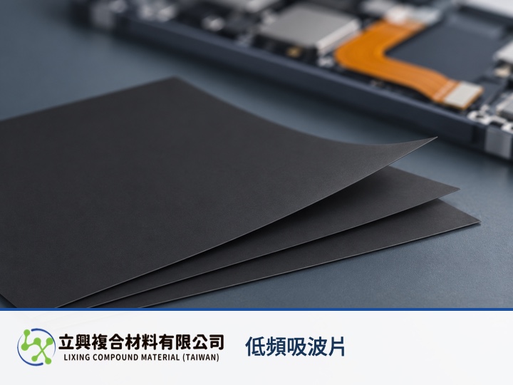
Tight mobile-device and high-compute layouts can still place absorbing material close to a noise source. The C-FO-LF Low-Frequency EMI Absorbing Sheet comes in 0.03–0.5 mm thicknesses, allowing engineers to narrow the grade by available gap, interference band and placement before device-level verification. Its thin, flexible form suits constrained locations near mobile FPCs, above CPUs and inside shield-can cavities.
Thin grades bring the absorber closer to the source
A range starting at 0.03 mm gives designers options around FPCs, chip tops and shield cavities. The official page specifies 0.03–0.5 mm with a ±10% thickness tolerance. Sampling should account for the sheet, adhesive, assembly clearance and component tolerance together.
Thickness must be evaluated with the noise band
C-FO-LF is listed for 10MHz–6GHz, with permeability μ' of 180 ± 20 at the page's stated 1MHz test condition. These values help define candidates but do not replace near-field probing or system measurements. Placement above an FPC, over a CPU or inside a shield can changes the coupling path and may change the result.
Flexibility supports constrained placements
The resin-based composite remains flexible for surfaces with limited installation room. The official applications include FPC noise suppression, CPU radiation reduction, smartphone SAR optimization and resonance control inside metal shielding frames. Each use still requires validation at the actual spectrum and location.
An engineering model links thickness and frequency
A peer-reviewed study uses the quarter-wavelength relation: t_m = n c / (4 f_m sqrt(|mu_r| |epsilon_r|)), n = 1, 3, 5, .... Here, t_m is matching thickness, c is the speed of light, f_m is matching frequency, and mu_r and epsilon_r are the magnitudes of relative complex permeability and permittivity. The published model is a conceptual tool for a conductor-backed absorber under approximately normal plane-wave incidence. Real electronics have near fields, complex geometry, adhesive layers, gaps and oblique incidence, so the formula does not guarantee this product's performance.
Compare adjacent grades under matched conditions
- Record the dominant noise frequencies and probe location.
- Provide the available gap, bonding area and bend requirement.
- Compare two adjacent thickness grades with the same assembly and measurement setup.
When an FPC or CPU area has little clearance, the 0.03–0.5 mm choices let the mechanical envelope guide the first sample set. Review the official C-FO-LF specifications and share the noise band, available gap and placement to discuss suitable sample grades.