
Copper Foil Self-Adhesive Tape Spreads Mobile-Device Hotspots in a Thin Profile
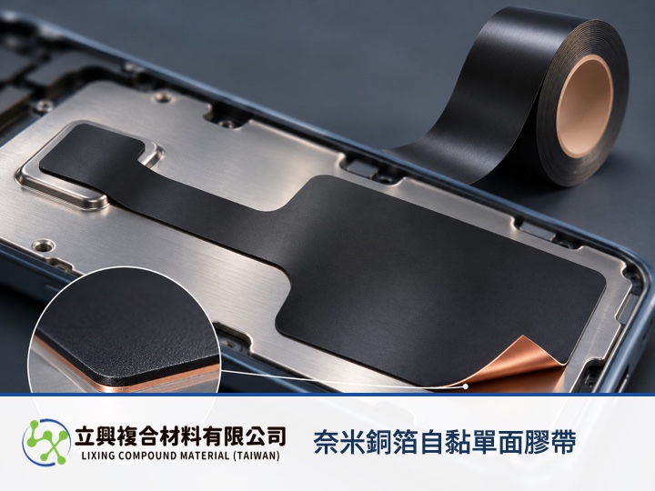
Copper Foil Self-Adhesive Single-Sided Tape can connect a localized hotspot to a larger spreading area within the tight stack of a phone or tablet. Selection should account for total thickness, available bonded area, interface flatness, and the conductivity data of the actual grade. The listed copper base, nano-carbon composite surface, and acrylic adhesive suit precision electronics that need thin bonding, heat spreading, and an EMI shielding path.
A thin tape leaves room for the device stack
The roll format supports a continuous path through narrow assemblies. The official page lists a total-thickness range of 0.03 ± 0.005 to 0.155 mm and a substrate range of 0.009 to 0.07 mm; available thickness and tolerance still require grade confirmation. The material is listed for smartphones, tablets, and precision electronics and can be die-cut to a defined outline.
The copper base spreads heat over a larger area
Available area around a hotspot is limited, so the useful function is a continuous solid conduction path. The product page lists 400 W/m·K for the base layer and 600 to 800 W/m·K for the composite layer. These are product-page values, not a device-level temperature reduction. Adhesive resistance, bonded area, and boundary cooling remain part of the design. The related article on thin electronic assembly covers the space constraint from a separate angle.
The adhesive keeps the path on the intended surface
The acrylic adhesive can bond the foil to listed surfaces such as stainless steel and aluminum. The page calls for a clean, dry surface, preheating below 15°C, and pressure that removes trapped air. Those conditions affect interface continuity. The official specification page also lists peel, initial tack, and holding-power ranges, so a sample request should identify the substrate and bonding condition.
One thin sheet can serve thermal and EMI layouts
The product page lists EMI shielding among the applications, which can help when a compact assembly must coordinate thermal and electromagnetic paths. System shielding still depends on grounding, overlap, and enclosure construction. Thermal contact and EMI contact locations should therefore be verified separately before the die-cut outline is frozen.
Fourier's law explains heat flow down a temperature gradient
NASA technical material gives the one-dimensional conduction relation Q_dot = -k A (dT/dx). Q_dot is heat-transfer rate in W, k is thermal conductivity in W/(m·K), A is area normal to heat flow in m², and dT/dx is the temperature gradient in K/m. The negative sign indicates flow toward lower temperature. The model applies to a conduction-dominated solid treated as a continuum. It omits adhesive contact resistance, voids, anisotropy, transient heat capacity, and device boundaries, so listed conductivity cannot directly predict a phone's temperature drop. Source: NASA Introduction to Numerical Methods in Heat Transfer.
Send the hotspot map with the sample request
Useful sample information includes hotspot and spreading-surface locations, available outline, maximum stack thickness, substrate, operating temperature, and any EMI-path requirement. Lixing does not offer online checkout. Use the product page to review the listed data and request a sample; the confirmed grade and technical data govern the final specification.